Building Circuit Simulations within LogicPlot
In this section, we will build a circuit of a full adder exploring the different stages of building a live circuit within the LogicPlot simulator. We will start off by creating a circuit of a half adder and insert it as a subcircuit to create a 4-bit full adder.
Create and Save New Project
The LogicPlot simulator backs up the circuit you are working on periodically and can restore it with Project → Recover Project, but you should still save your project under a name so that you can reopen it later.
Follow the below steps to create a new project and save it:
-
Open the LogicPlot home page and click on the Launch Simulator button to launch the simulator. Refer Figure 7.1.
 Figure 7.1
 -
Navigate to the Quick Access Panel and click on the Save icon, or choose Project → Save Offline. The Enter Project Name pop-up window is displayed. Refer Figure 7.2.
NOTE: A project saved this way is stored in your browser's local storage and listed under Project → Open Offline. To keep a copy as a file, or to move a project to another machine, use Project → Export as File.
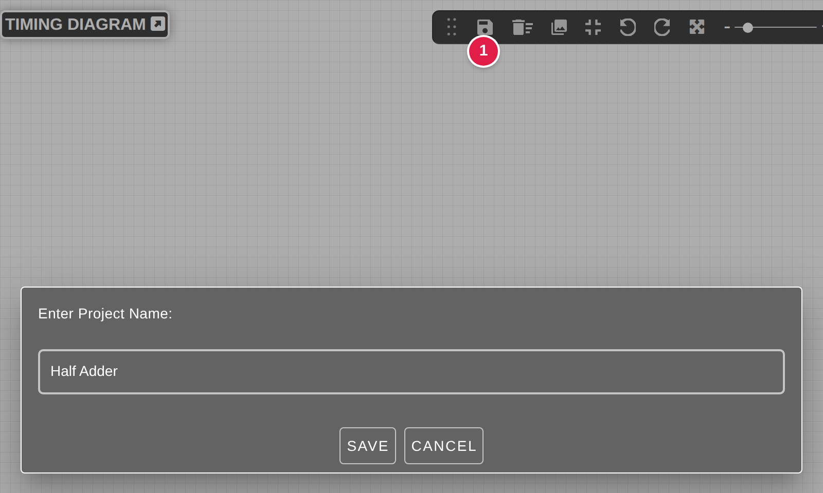 Figure 7.2
 -
Enter a name and click OK. The project name now appears in the menu bar (refer Figure 7.3).
 Figure 7.3
 -
To share the project or keep a backup, choose Project → Export as File and download the
.cvfile (refer Figure 7.4). Anyone can open it with Project → Import Project.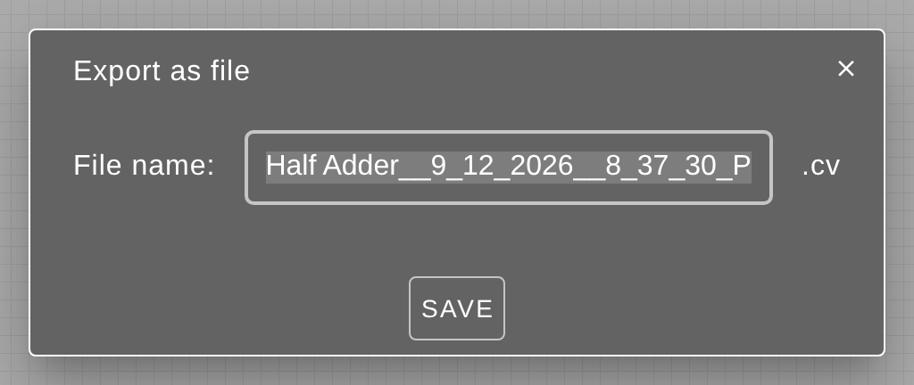 Figure 7.4
Create Circuit Using LogicPlot Simulation
Follow the below steps for creating a half adder circuit within the LogicPlot simulator:
-
Navigate to the CIRCUITS ELEMENTS panel. Identify the relevant circuit elements and drop them on the canvas. If required, you may search for an element in the search bar. Refer Figure 7.5.
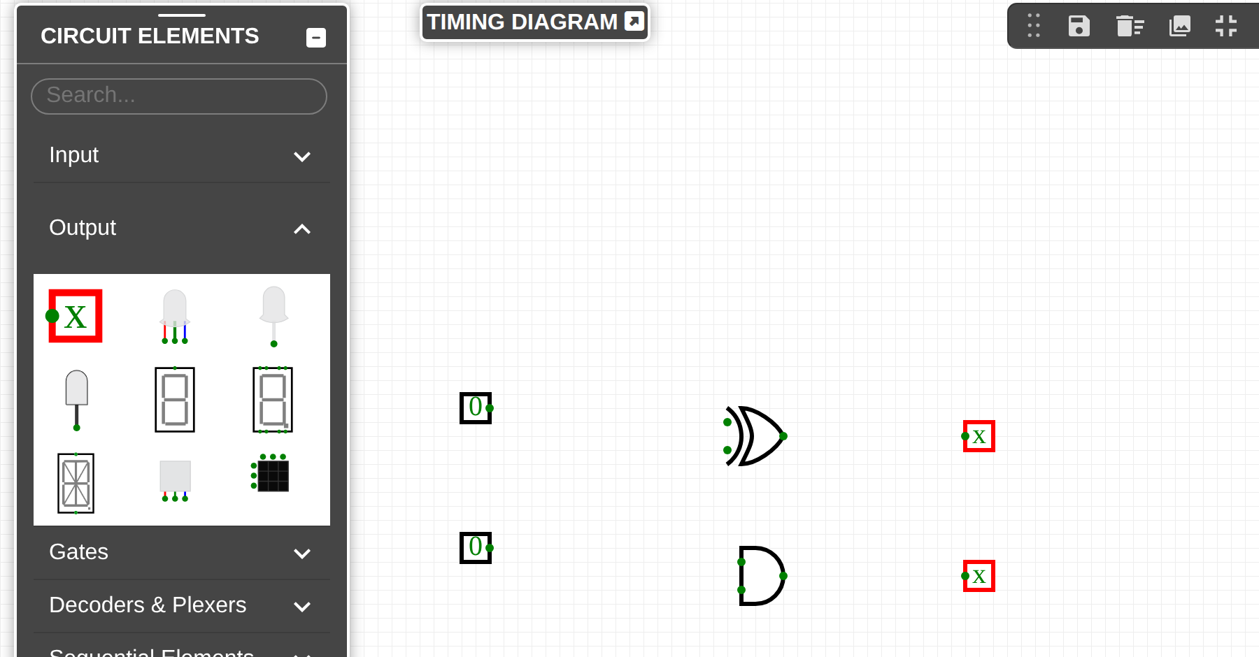 Figure 7.5
 -
Connect the circuit elements by clicking on one node and dragging the mouse to the other node. Refer to Figure 7.6 for the final circuit connection.
TIP: Hold down Ctrl key. Click on a node and simply move the cursor to the final node to which it needs to be attached. Clicking on the wire will insert a node at that position. Upon reaching the final node, leave the Ctrl key and click on the node to end the wire.
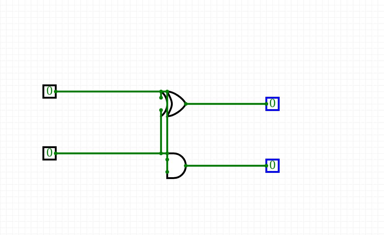 Figure 7.6
 -
Select a circuit element. It will be highlighted in yellow as shown in Figure 7.7.
-
Navigate to the PROPERTIES panel. Edit the Label parameter to add a label for the selected circuit element. Refer Figure 7.7.
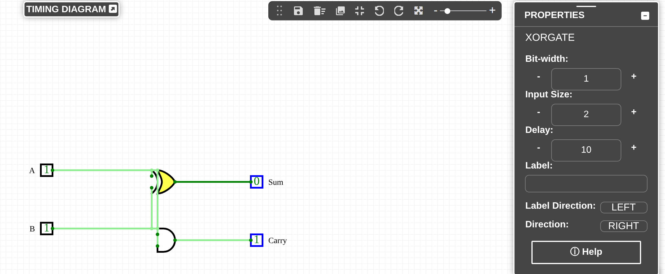 Figure 7.7
 -
Repeat steps 7 and 8 to add labels for the remaining circuit elements as shown in Figure 7.7.
Edit Circuit Layout
Before inserting a circuit as a subcircuit, the circuit layout must be edited to prevent any loss of wiring connections across different nodes or ports in the integrated circuit schematic may be lost.
Follow the below steps to view and edit the circuit layout of the half-adder circuit:
-
Navigate to the PROPERTIES panel.
-
Click on the Edit Layout button to display the circuit layout for the built circuit (refer Figure 7.8).
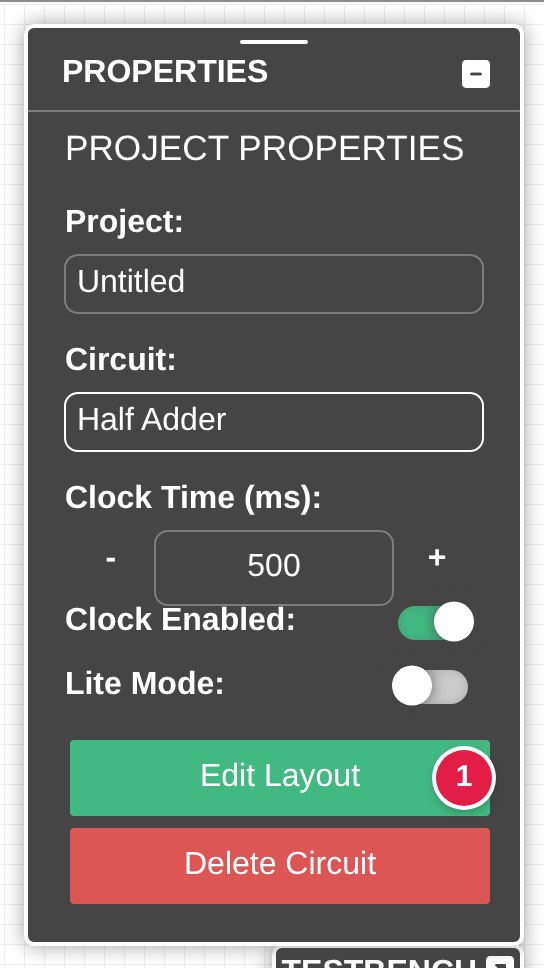 Figure 7.8
 -
The Edit Layout screen displays the page as shown in Figure 7.9. The circuit is placed inside a back box. The LAYOUT panel displays different options for editing the layout of the circuit.
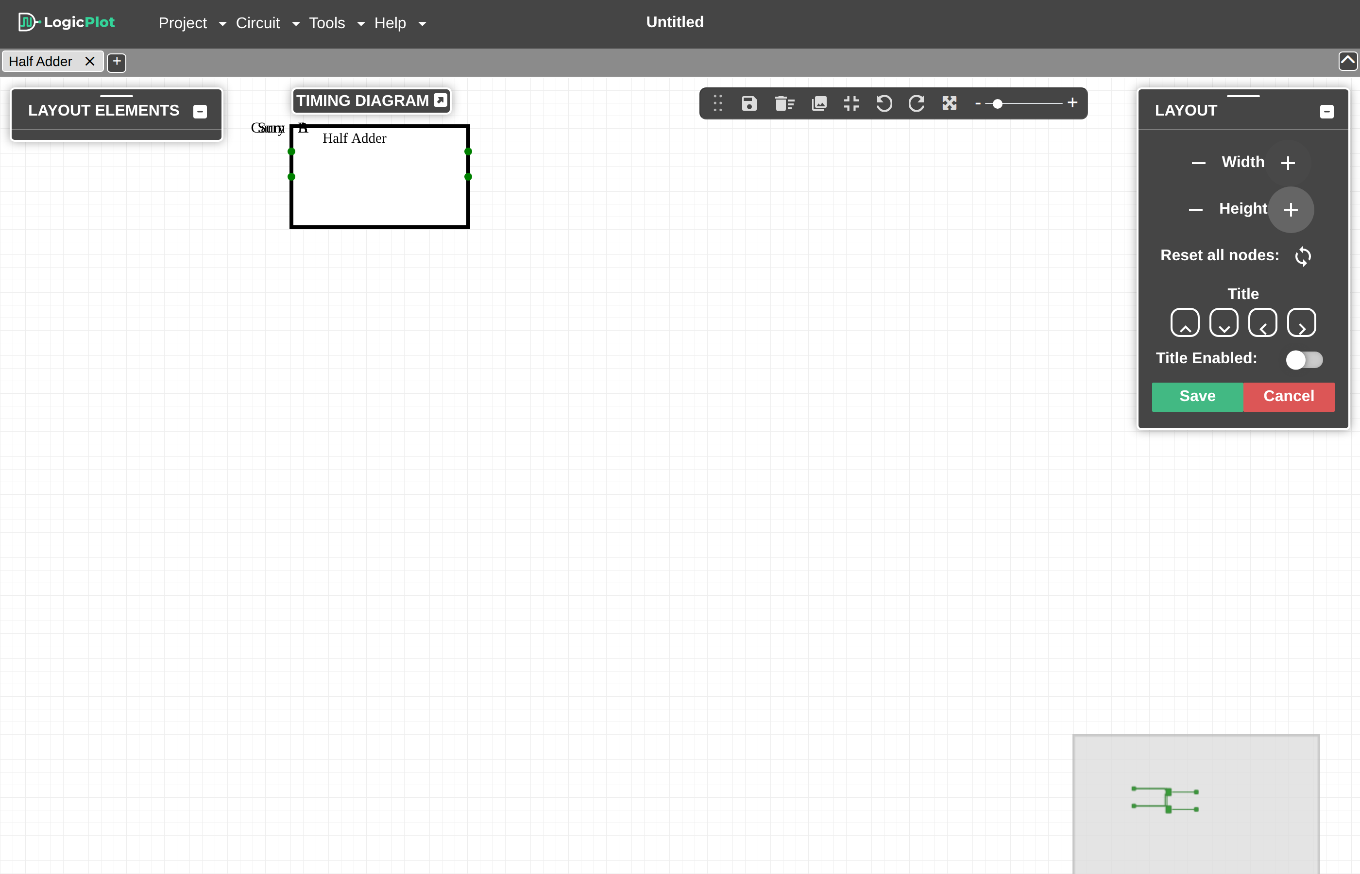 Figure 7.9
 -
Change the desired settings of the LAYOUT panel.
-
Click Save to save the layout settings as shown in Figure 7.10.
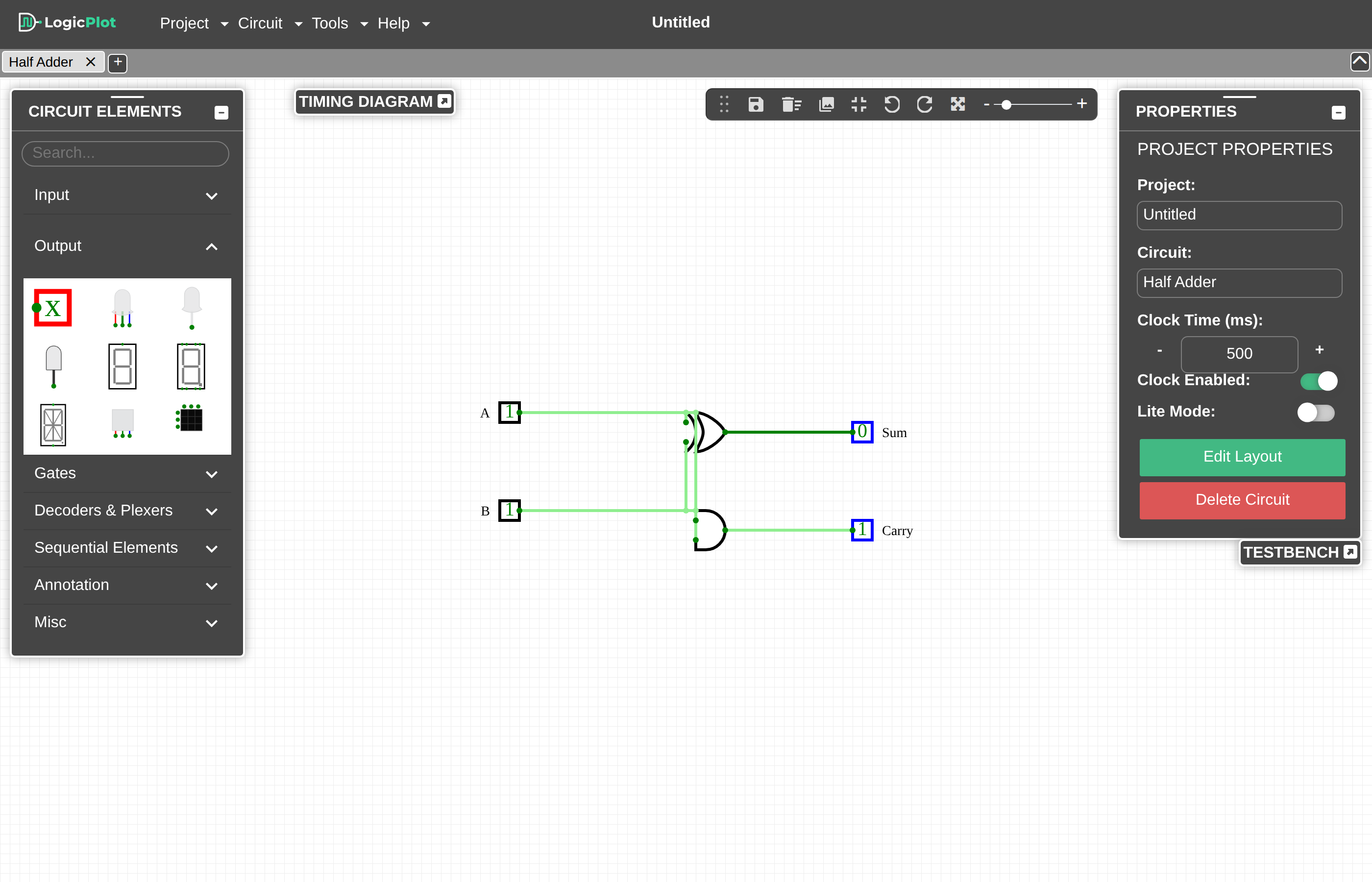 Figure 7.10
Insert Subcircuit
Subcircuits can be nested across other circuit tabs as a LogicPlot simulation or as a Verilog module. This section lists the different steps for inserting subcircuits generated as a LogicPlot simulation or as a Verilog code.
a. Insert Subcircuit as a LogicPlot Simulation
Follow the below steps for building a full adder circuit using two half-adder subcircuits:
-
Click on the add tab icon (refer Figure 7.11) displayed in the circuit tab section. Alternatively, you may also click on NewCircuit+ selection in the Circuit drop-down menu. As shown in Figure 7.11, the Enter circuit name: pop up window is displayed.
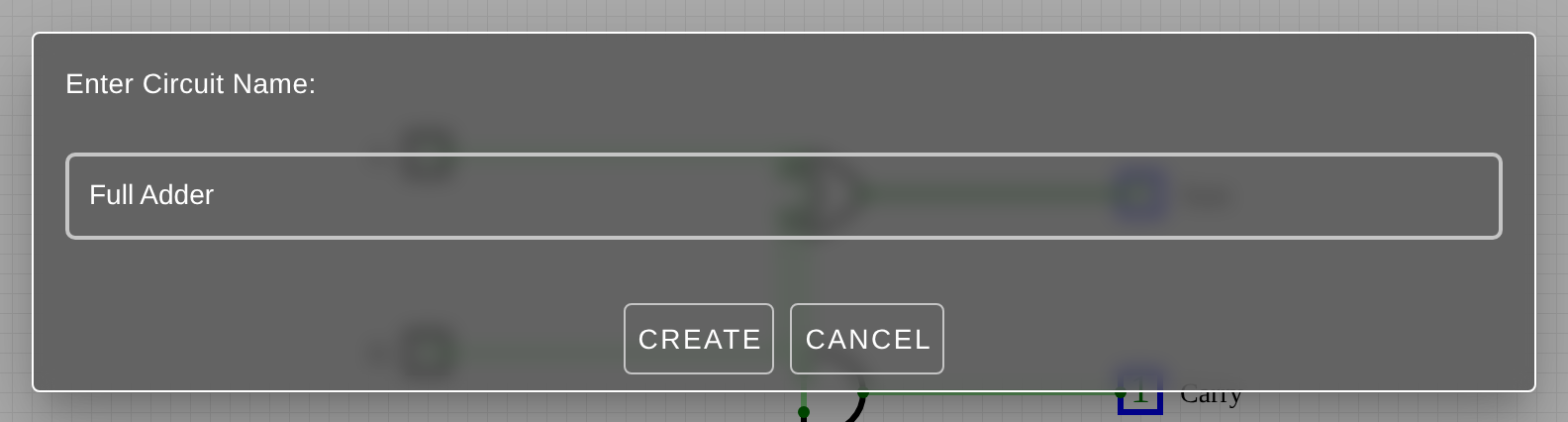 Figure 7.11
 -
Enter a circuit name in the text field as shown in Figure 7.11.
-
Click OK to save the circuit name. Refer Figure 7.12.
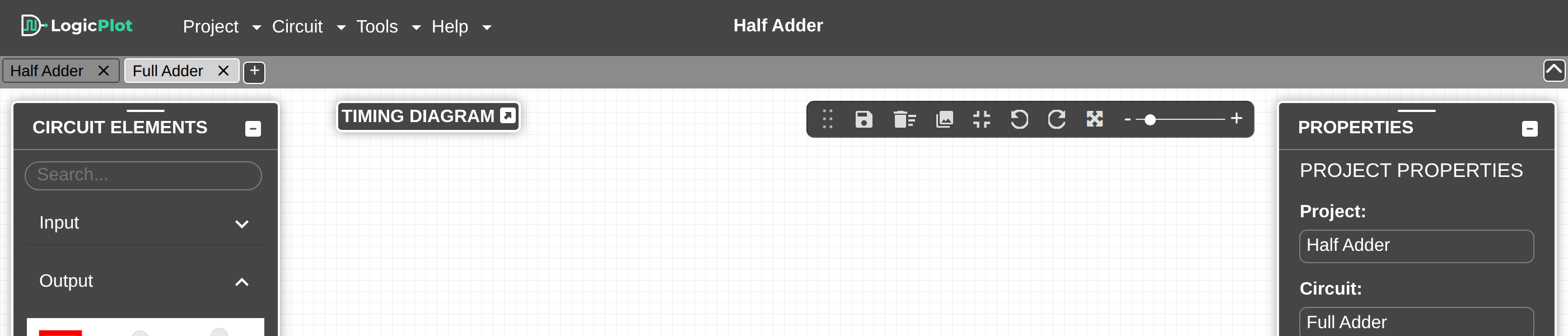 Figure 7.12
 -
Navigate to Circuit drop-down menu to select Insert SubCircuit from the drop down menu. As shown in Figure 7.13, the Insert SubCircuit pop up window is displayed.
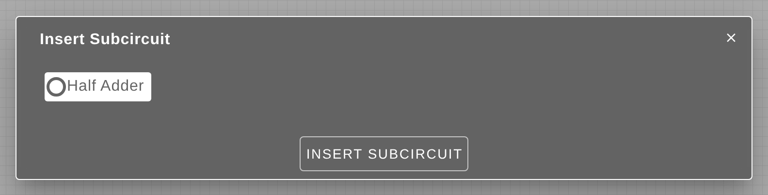
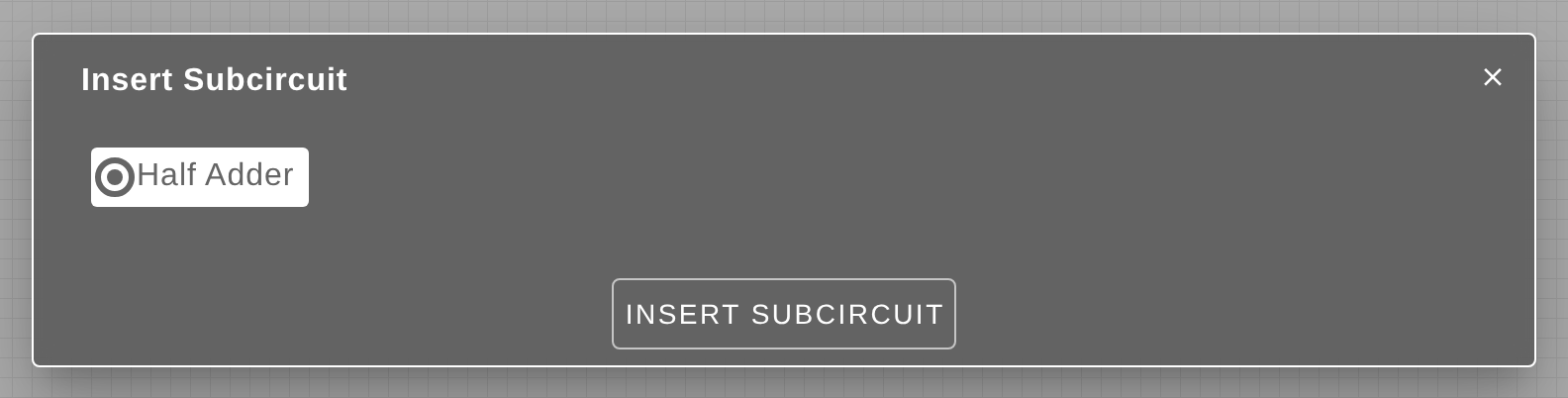
- Select the circuit that you wish to insert. Refer Figure 7.14.
-
Click the Insert SubCircuit button to insert the subcircuit within the Full Adder tab (refer Figure 7.14).
-
Repeat the steps from 15 to 20 to add more sub-circuits to your circuit.
TIP: Duplicate any circuit by selecting the circuit (CTRL + A), copy the circuit (CTRL + C) and paste the circuit (CTRL + V) in the desired tab or another project file.
-
Refer to Figure 7.15 and complete the wiring connections of the full adder circuit.
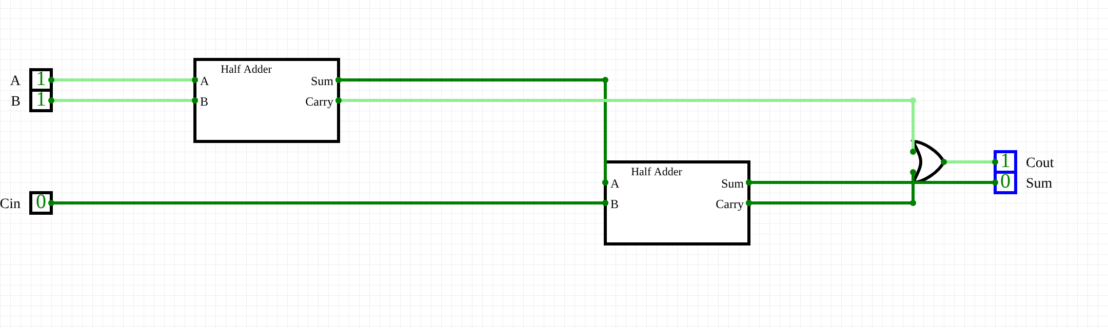 Figure 7.15
b. Insert Circuit Using Verilog Module
If required, a user can also insert a Verilog module as a subcircuit. Follow the below steps to insert a circuit layout constructed using a verilog module:
-
Navigate to Circuit drop-down menu to select New Verilog Module from the drop down menu. As shown in Figure 7.16, the Enter circuit name pop up window is displayed.
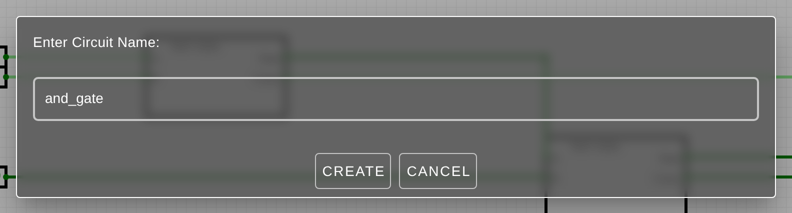 Figure 7.16
 -
Enter a circuit tab name in the text field. Refer Figure 7.16.
-
Click **OK **to launch the Verilog code interface window as shown in Figure 7.17.
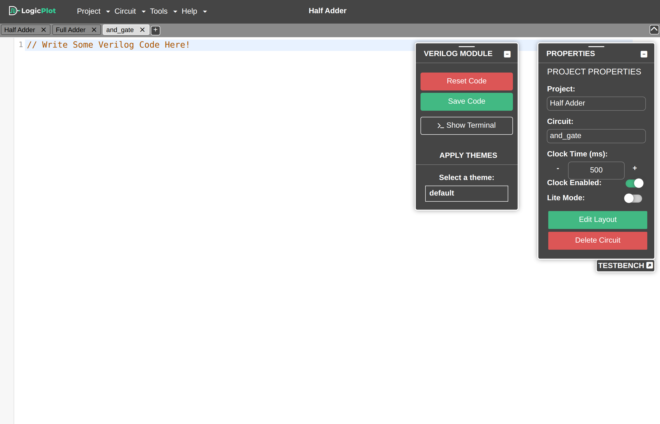 Figure 7.17
 -
Enter the desired Verilog code in the module interface. Refer Figure 7.18.
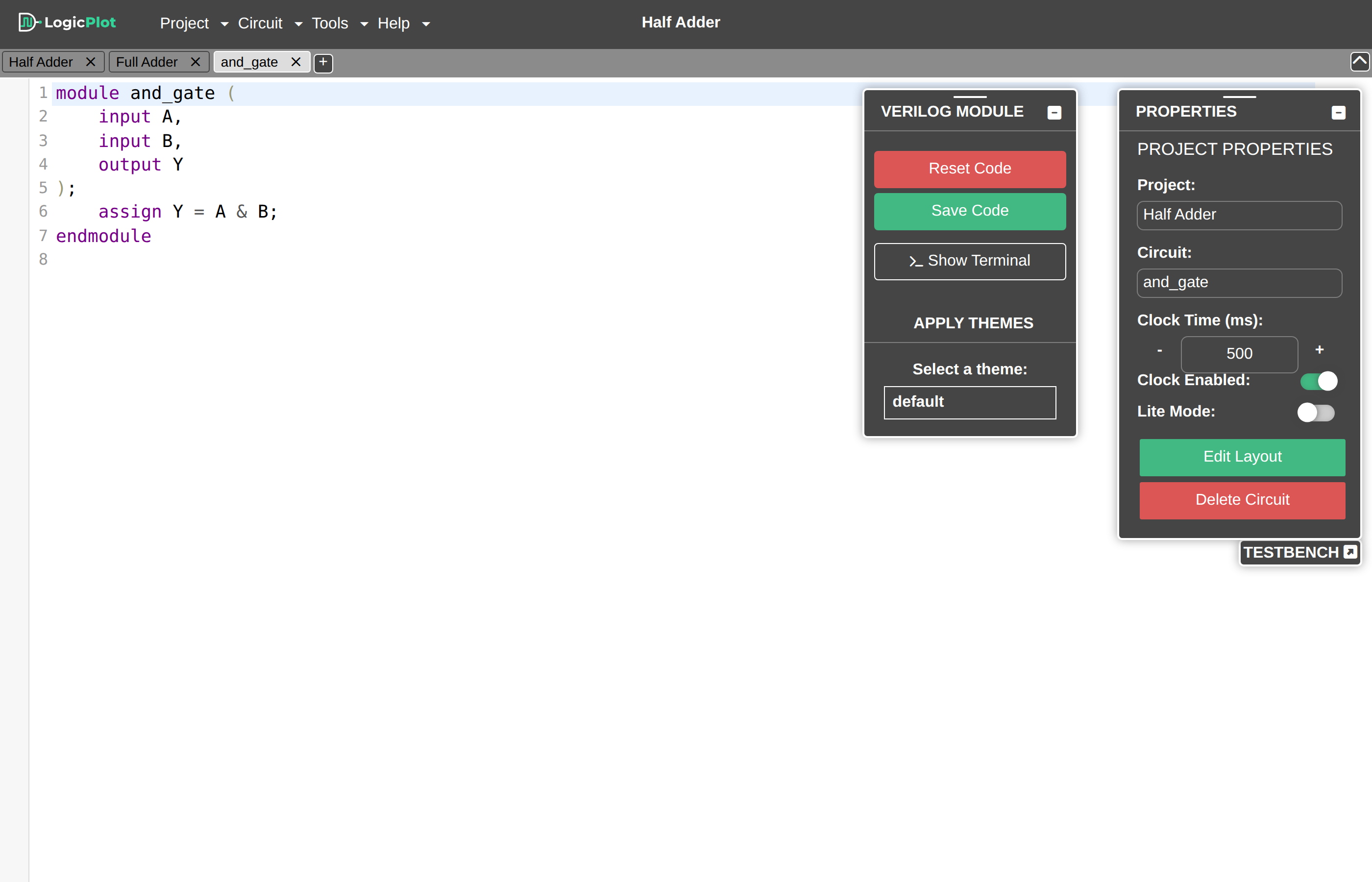 Figure 7.18
 -
Click on the Save Code button to receive the message that the code has been saved successfully. Refer Figure 7.19.
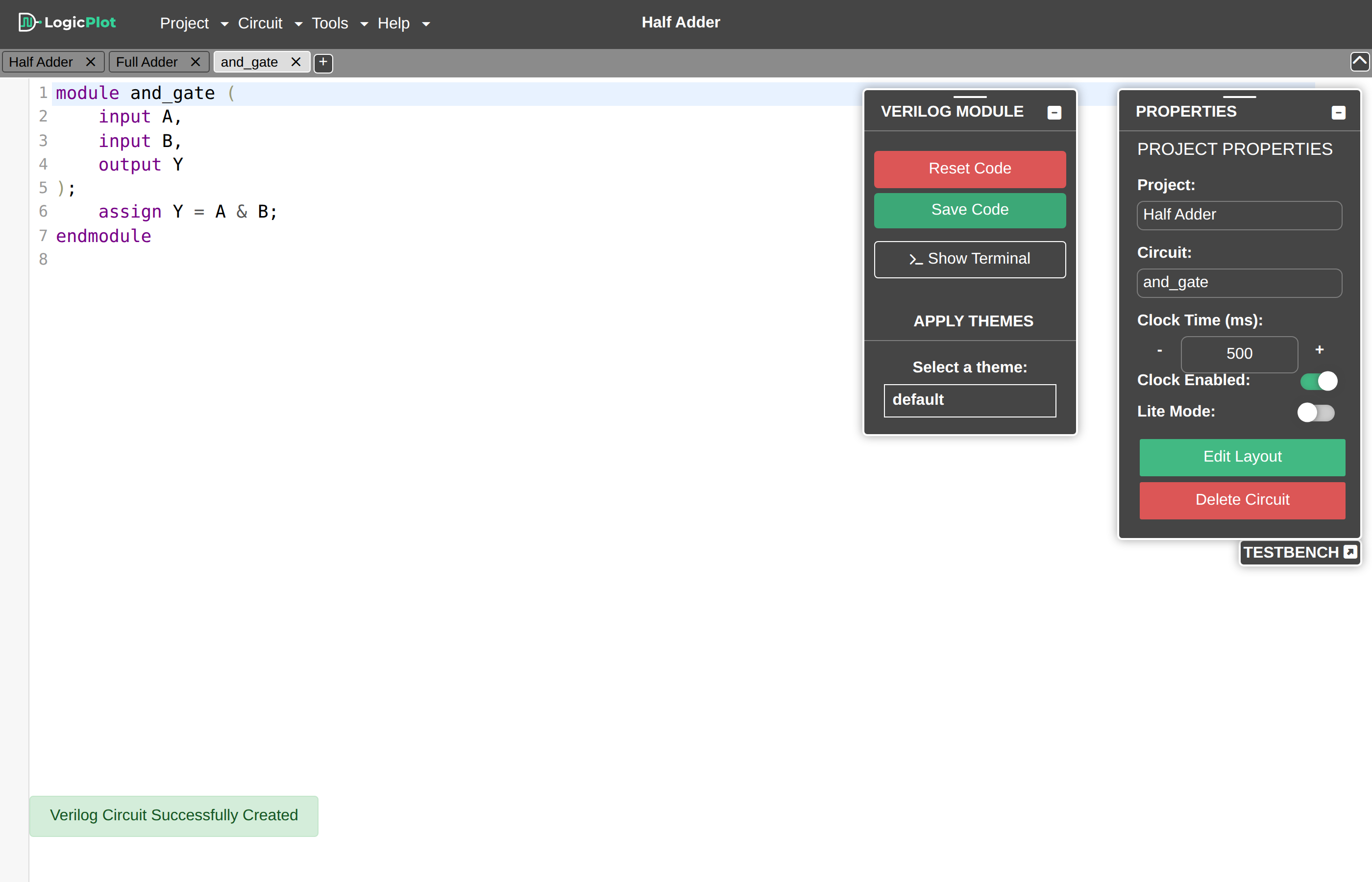 Figure 7.19
Annotate Circuit
Follow the below steps to annotate the final circuit diagram:
-
Navigate to the Misc section of the CIRCUIT ELEMENTS panel as shown in Figure 7.20.
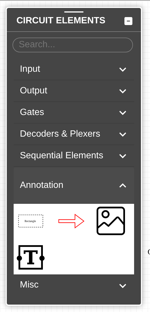 Figure 7.20
 -
Drag the Text Tool element on the canvas as shown in Figure 7.21.
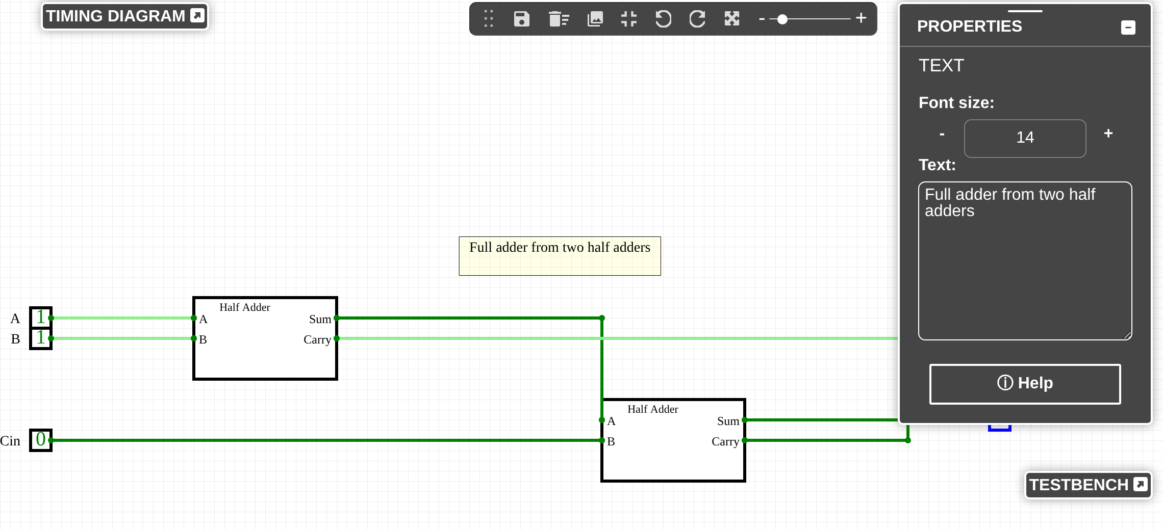 Figure 7.21
 -
Navigate to the PROPERTIES panel to edit the Label: text field as shown in Figure 7.21.
-
Repeat steps 24 to 26 to add more annotation elements. In Figure 7.22, a Rectangle Tool element has been added to highlight the structural relationship across different elements .
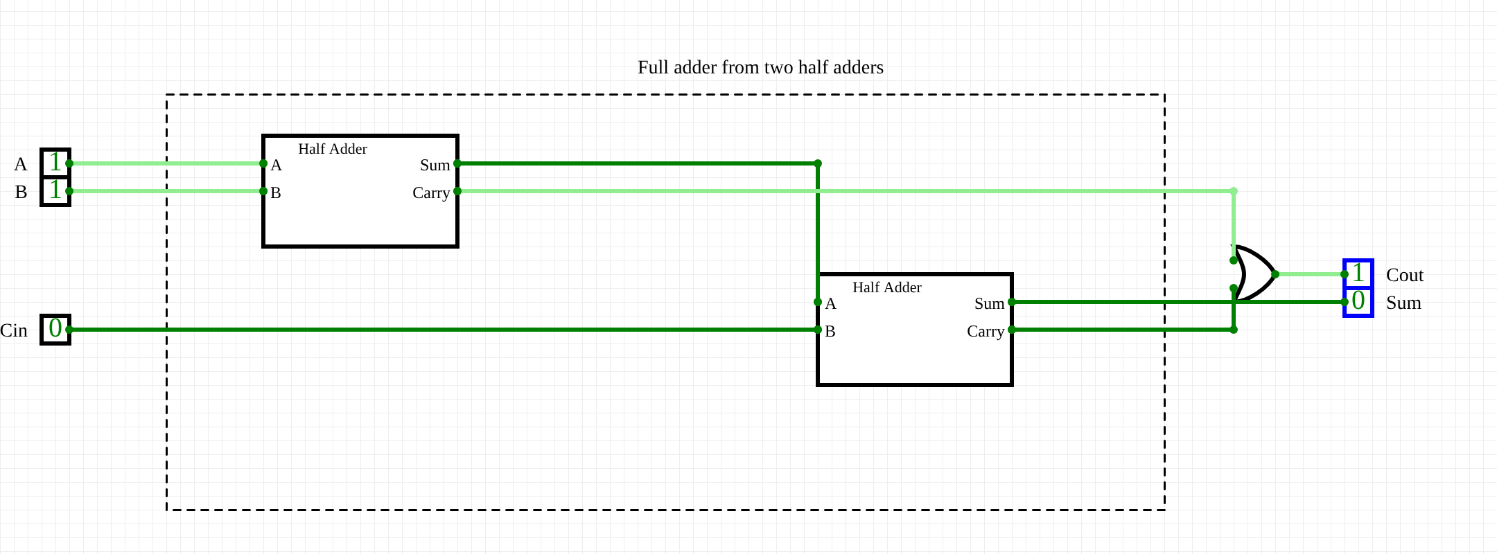 Figure 7.22