Timing Diagram
A timing diagram is used for analyzing and debugging the behavior of circuits for different input sequences. Using the Flag circuit element, timing diagrams can be used to debug logical mistakes and race conditions. Additionally, this can be used to explain different concepts such as propagation delay, stable state and race conditions.
Note: The timing diagram may not be accurate if used with both clock and user input. Ideally the circuit should be driven completely by the clock or completely driven by user input.
Similar to other panels available in the LogicPlot simulator, the TIMING DIAGRAM panel is collapsible and can be dragged by the mouse. Figure 6.2 elucidates the different icons available on the TIMING DIAGRAM panel for plotting a waveform.
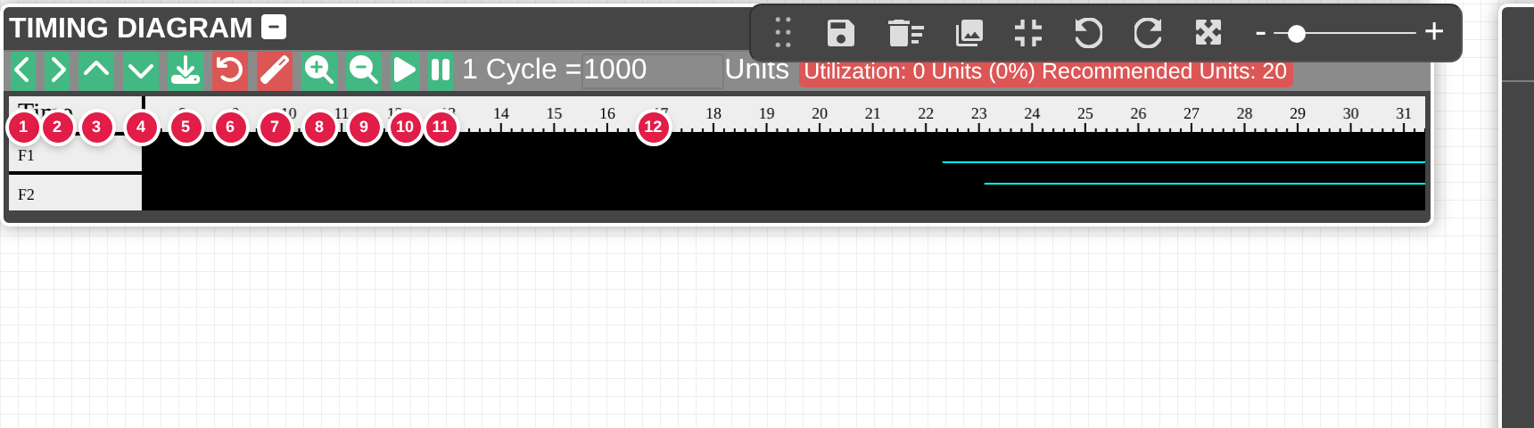
Table 6.1: Icons on the TIMING DIAGRAM panel (numbered as in Figure 6.2)
| No. | Icon | Description |
| 1 | Decrease size | Narrows the plot so more cycles fit in the panel. |
| 2 | Increase size | Widens the plot for a closer look at each cycle. |
| 3 | Decrease height | Makes each signal row shorter. |
| 4 | Increase height | Makes each signal row taller. |
| 5 | Download as image | Saves the current waveform as an image file. |
| 6 | Reset | Clears the recorded waveform and starts plotting again. |
| 7 | Auto calibrate | Sets the number of delay units per cycle from the circuit's critical path. |
| 8 | Zoom in | Zooms into the time axis. |
| 9 | Zoom out | Zooms out of the time axis. |
| 10 | Resume auto-scroll | Keeps the newest samples in view as the simulation runs. |
| 11 | Pause auto-scroll | Stops the plot from scrolling so a region can be inspected. |
| 12 | 1 Cycle = ___ Units | Number of simulation delay units mapped to one half clock cycle (see below). |
Mapping Delays While Using Timing Diagram
In order to visualize a timing diagram, it is necessary to map the simulation delay units in a single half clock cycle. This is done by setting “1 cycle = ___ units” (refer Figure 6.2, item 12). While this number can be set auto calibrated by clicking on the Auto Calibrate icon in the TIMING DIAGRAM panel, this number must exceed the delay in the critical path of the circuit.
Similarly, the clock interval maps how many milliseconds are there in one half clock cycle. As explained below, the delays can also be indirectly mapped to time.
- 1 clock cycle --> 500 ms
- 1 clock cycle --> 50 units
- 1 unit --> 10 ms
Understanding Circuit Behavior Using Timing Diagram
Figure 6.3 illustrates a circuit design where two NOT gates cancel out each other to behave as an XNOR gate.
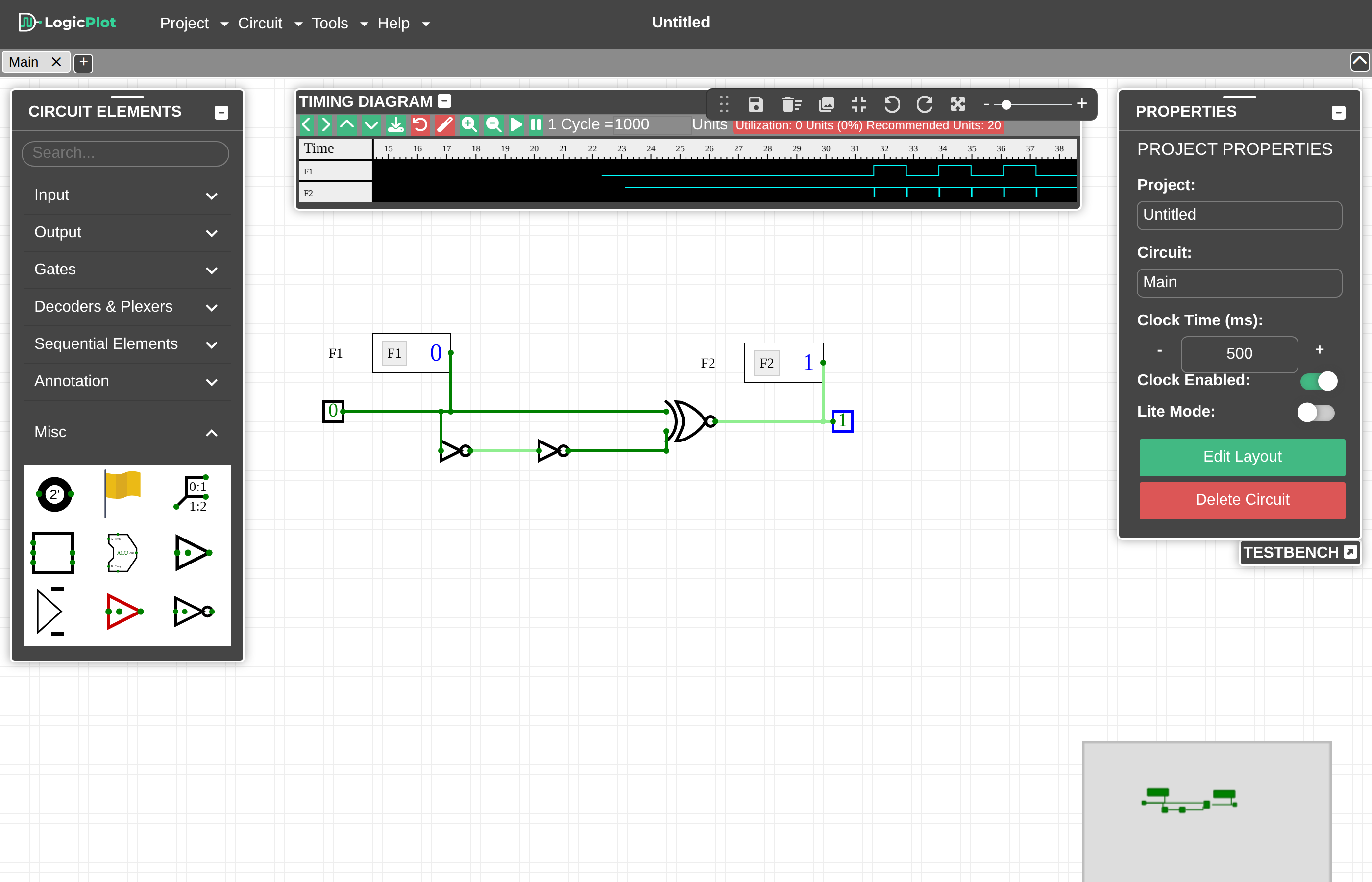
Reading TIMING DIAGRAM panel: The delay has been set to 1 clock cycle = 50 units. So each unit is 2% of a clock cycle. Therefore, 10 units is 20% of a clock cycle.
- 1 clock cycle --> 500 ms
- 1 clock cycle --> 50 units
- 1 unit --> 10 ms
Visualizing circuit behavior using the TIMING DIAGRAM panel: The two NOT gates cancel out each other to behave as an XNOR gate. Thus, irrespective of the input set, the output must be 1. However, the TIMING DIAGRAM panel shows that after 10 units of time, flag F1 moves from 0 -->1. After an additional 10 units of time, flag F2 goes to 0. This happens because the first input of XNOR gate becomes 1 but the second input is still 0 (due to NOT gate delays). After an additional 20 units of NOT gate delay, the circuit becomes stable and flag F2 goes back to 1.
- Time = 0 | F1 = 0, F2 = 1 (stable state)
- Time = 10 | F1 = 1, F2 = 1 (unstable state)
- Time = 20 | F1 = 1, F2 = 0 (unstable state - glitch) (XNOR delay)
- Time = 40 | F1 = 1, F2 = 1 (stable state) (2 NOT gates + XNOR delay)