Misc
- ALU
- Adder
- Subtractor
- Comparator
- Arithmetic Elements
- Buffer
- Controlled Inverter
- TriState Buffer
- Tunnel
- Splitter
- Equal Split
- Unequal Split
- Flag
- Two's Complement
ALU
An Arithmetic Logic Unit (ALU) circuit element is a combinational digital electronic circuit that performs arithmetic and bitwise operations on integer binary numbers. Figure 4.15 highlights the different ports in the ALU circuit element available within LogicPlot and Table 4.19 provides a brief description of the different ports.
Properties that can be customized in the PROPERTIES panel include: Direction, BitWidth
Table 4.19: Brief description of the ALU circuit element ports
| Name | Description |
| A | Receives an input operand |
| B | Receives an input operand. |
| CTR (BitWidth 3) | Receives an input operand with bit width of 3 bits. |
| Ans | Generates the output after the operation on the received input operands has been completed. |
| Carry | Generates the carry output after the operation on the received input operands has been completed. |
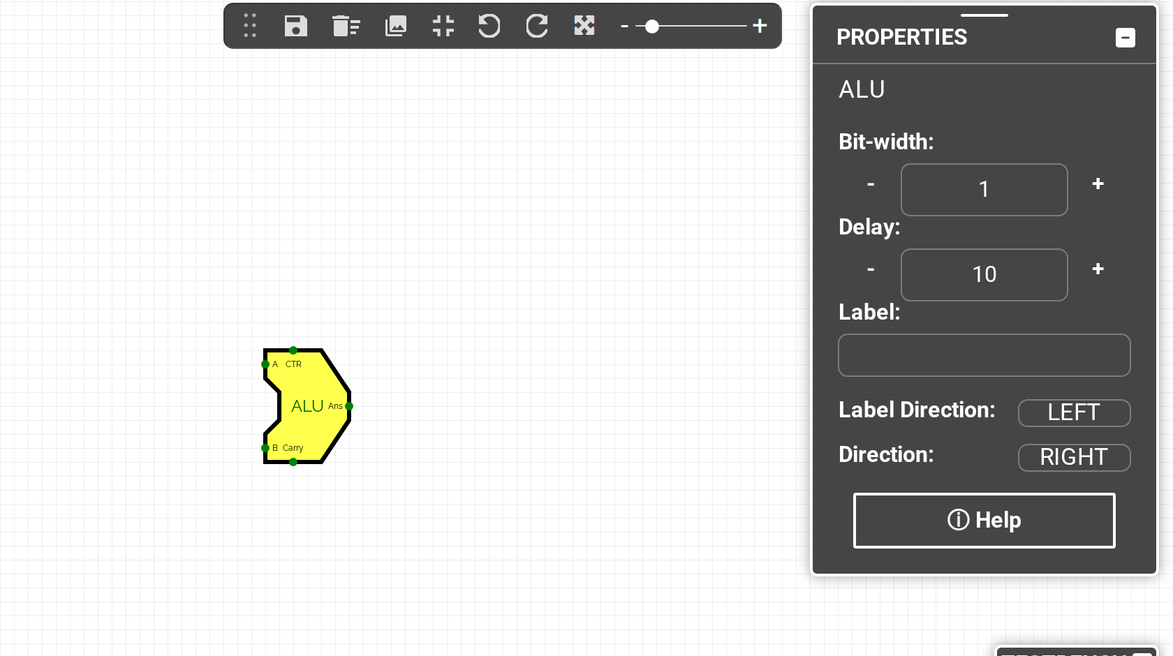
As required, the users may change the orientation of the ALU circuit element by editing the Direction attribute available for the ALU circuit element in the PROPERTIES panel (refer Figure 4.17). Alternatively, users can use the arrow keys on their keyboard to change the orientation.
In the embedded circuit below, A and B are two operands.Table 4.20 displays the opcodes for different ALU functionalities.
Note: SLT (Set Less Than): If A is less than B, output is 1 else output is 0.
Table 4.20: CTR port input opcodes for different functionalities of ALU
| Opcode | Opcode Value | Operation |
| 0 0 0 | 0 | A & B |
| 0 0 1 | 1 | A | B |
| 0 1 0 | 2 | A + B |
| 1 0 0 | 4 | A & ~B |
| 1 0 1 | 5 | A | ~B |
| 1 1 0 | 6 | A - B |
| 1 1 1 | 7 | SLT |
Adder
The Adder circuit element is a logical circuit of a full adder that performs an addition operation on binary numbers and produces a sum of the three inputs and a carry value (Cout). Figure 4.18 displays the different pins available for the **Adder **circuit element within LogicPlot and Table 4.21 shares a brief description of the same.
Properties that can be customized in the PROPERTIES panel include: Direction
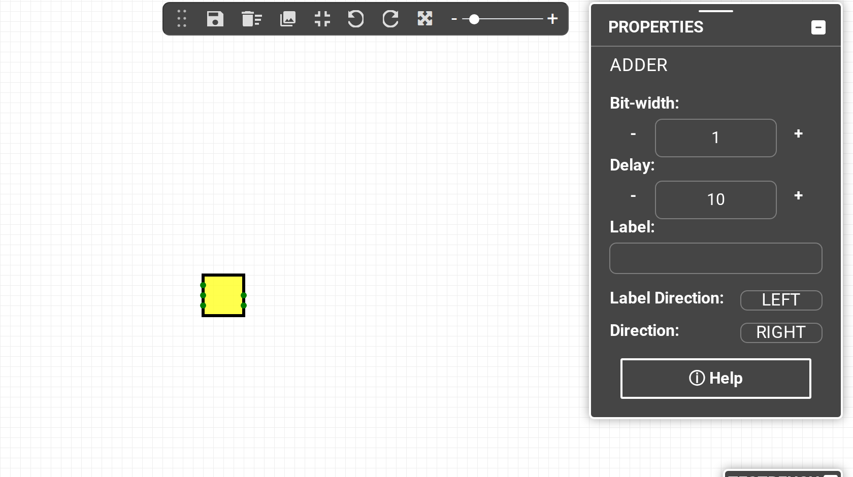
Table 4.21: Brief description of the Adder circuit element
| Name | Description |
| A | Receives an input operand |
| B | Receives an input operand. |
| Cin | Receives an input carry value operand |
| Sum | Generates the output after the operation on the received input operands. ((A XOR B) XOR Cin) |
| Cout | Generates the carry left over after the output operation has been completed. ((A AND B) OR (Cin AND (A XOR B) ) |
Using Table 4.22, you can verify the behavior of the Adder circuit element in the live circuit embedded below:
Table 4.22: Truth Table for an adder
| A | B | Cin | SUM | Cout |
| 0 | 0 | 0 | 0 | 0 |
| 0 | 0 | 1 | 1 | 0 |
| 0 | 1 | 0 | 1 | 0 |
| 0 | 1 | 1 | 0 | 1 |
| 1 | 0 | 0 | 1 | 0 |
| 1 | 0 | 1 | 0 | 1 |
| 1 | 1 | 0 | 0 | 1 |
| 1 | 1 | 1 | 1 | 1 |
Subtractor
The Subtractor circuit element computes A − B − Bin on unsigned binary numbers and reports whether a borrow was needed. It is the counterpart of the Adder for building ALUs, counters that count down and magnitude circuits. Figure 4.25 displays the pins of the Subtractor and Table 4.22a describes them.
Properties that can be customized in the PROPERTIES panel include: Direction, BitWidth
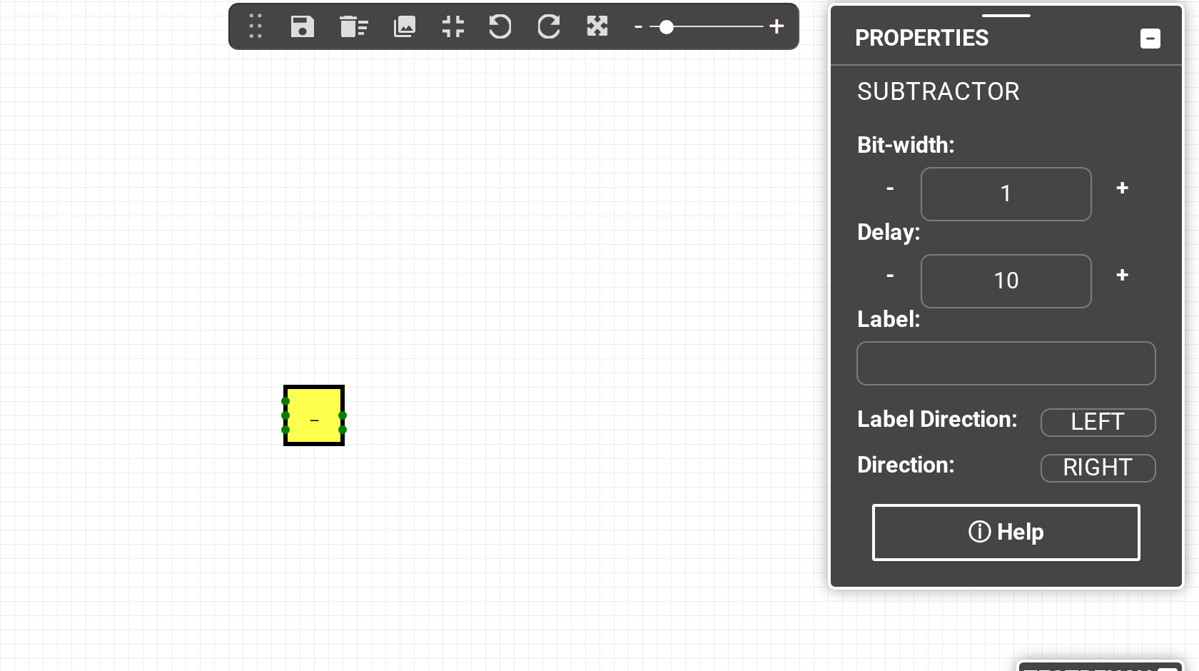
Table 4.22a: Brief description of the Subtractor circuit element
| Name | Description |
| A | Receives the minuend (the number subtracted from) |
| B | Receives the subtrahend (the number being subtracted) |
| Bin | Receives a 1-bit borrow in; treated as 0 when unconnected |
| Diff | Generates A − B − Bin, wrapped to the element's bit width |
| Bout | Goes high when A is smaller than B + Bin, that is, when the subtraction needs a borrow |
Table 4.22b: Truth table for a 1-bit subtractor
| A | B | Bin | Diff | Bout |
| 0 | 0 | 0 | 0 | 0 |
| 0 | 0 | 1 | 1 | 1 |
| 0 | 1 | 0 | 1 | 1 |
| 0 | 1 | 1 | 0 | 1 |
| 1 | 0 | 0 | 1 | 0 |
| 1 | 0 | 1 | 0 | 0 |
| 1 | 1 | 0 | 0 | 0 |
| 1 | 1 | 1 | 1 | 1 |
Chaining subtractors works like chaining adders: connect Bout of the lower stage to Bin of the next.
Comparator
The Comparator circuit element compares two unsigned numbers and raises exactly one of its three outputs: A<B, A=B or A>B. It replaces the web of XNOR gates that a hand-built magnitude comparator needs and is the natural companion of the Subtractor and ALU. Figure 4.26 displays the pins of the Comparator and Table 4.22c describes them.
Properties that can be customized in the PROPERTIES panel include: Direction, BitWidth
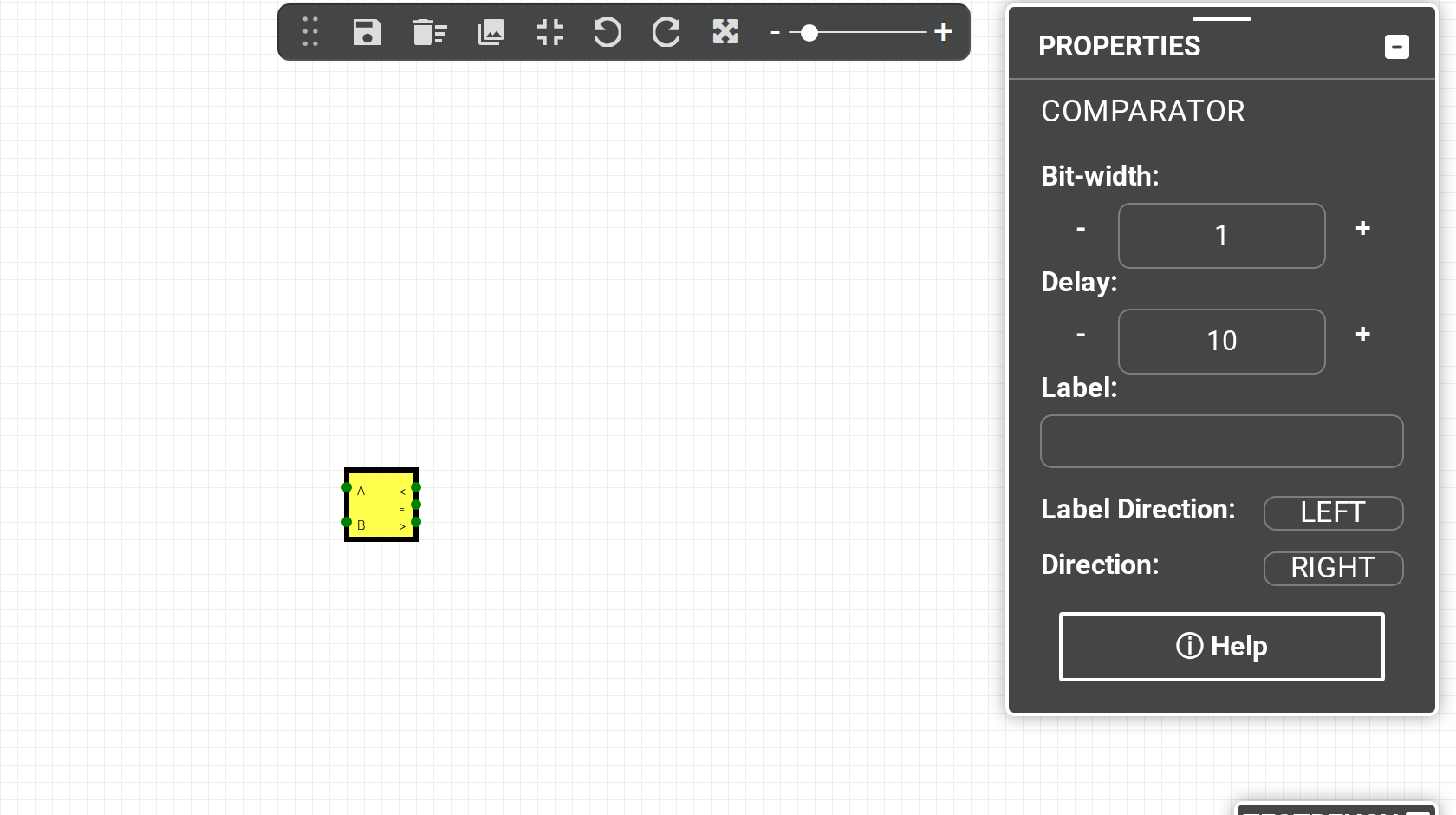
Table 4.22c: Brief description of the Comparator circuit element
| Name | Description |
| A | Receives the first operand |
| B | Receives the second operand |
| A<B | High when A is strictly smaller than B |
| A=B | High when both operands are equal |
| A>B | High when A is strictly greater than B |
Both inputs share the element's bit width, so an 8-bit comparator needs 8-bit inputs on A and B. Values are compared as unsigned numbers; to compare two's-complement values, invert the sign bit of both operands with a Splitter and an XOR gate first.
Arithmetic Elements
Next to the Adder, Subtractor and Comparator, the Misc category holds five word-level arithmetic elements that map directly onto Verilog operators. Each has a BitWidth for its inputs; the multiplier, divider and power also expose a separate Output BitWidth so that wide results are not truncated.
| Element | Inputs | Output | Verilog |
| Multiplier | A, B | Product | A * B |
| Divider | A, B | Quotient, Remainder | A / B, A % B |
| Power (Exponent) | A, B | Result | A ** B |
| Shift Left | A, Shift | Result | A << Shift |
| Shift Right | A, Shift | Result | A >> Shift |
These elements are also what the Verilog module importer produces for the matching operators, so a circuit built from them exports back to clean Verilog with Circuit → Export Verilog.
Buffer
The Buffer circuit element has only a single input and a single output. Its behavior is the opposite of a NOT gate––passes its input unchanged to its output. Table 4.23 displays the truth table of a buffer.
Properties that can be customized in the PROPERTIES panel include: Direction
Table 4.23: Truth table for a buffer
| Input | Output |
| 0 | 0 |
| 1 | 1 |
You can verify the behavior of the Buffer circuit element in the live circuit embedded below:
Controlled Inverter
The Controlled Inverter circuit element is a controlled gate that inverts the input signal when enabled. As illustrated in the circuit, this element includes an Enable input that controls whether the input is inverted at the output or the output is disconnected from the circuit.
- If the Enable input signal is HIGH, the controlled inverter gate inverts the input signal (behaves like a NOT gate).
- If the Enable input signal is LOW, the controlled inverter gate passes a high impedance signal which effectively disconnects its output from the circuit.
If required, a user can change the orientation of the circuit element using the arrow keys on the keyboard or editing the value of the Direction attribute available in the PROPERTIES panel for the Controlled Inverter circuit element.
Properties that can be customized in the PROPERTIES panel include: Direction, BitWidth
Table 4.24: Truth table for a Controlled Inverter gate
| Enable | Input | Output |
| 0 | 0 | Z |
| 0 | 1 | Z |
| 1 | 0 | 1 |
| 1 | 1 | 0 |
You can verify the behavior of the Controlled Inverter circuit element in the live circuit embedded below:
TriState Buffer
The TriState buffer circuit element behaves similar to a buffer. As Figure 4.17 illustrates, this circuit element includes an additional Enable input that controls whether the primary input is passed to its output or not.
- If the Enable input signal is HIGH, the tri-state buffer behaves like a normal buffer.
- If the Enable input signal is LOW, the tri-state buffer passes a high impedance signal which effectively disconnects its output from the circuit.
If required, a user can change the orientation of the circuit element using the arrow keys on the keyboard or editing the value of the Direction attribute available in the PROPERTIES panel for the TriState buffer circuit element.
Properties that can be customized in the PROPERTIES panel include: Direction, BitWidth
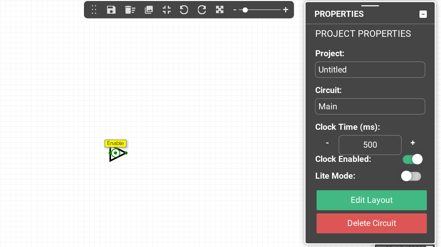
Table 4.25: Truth table for a TriState buffer
| Enable | Input | Output |
| 0 | 0 | Z |
| 0 | 1 | Z |
| 1 | 0 | 0 |
| 1 | 1 | 1 |
You can verify the behavior of the TriState buffer circuit element in the live circuit embedded below:
Tunnel
The Tunnel circuit element encapsulates desired connection points in a tunnel for transmitting signals without using a wire (refer Figure 4.18). It is recommended to use this circuit element for design areas that may require excessive wiring to connect otherwise.
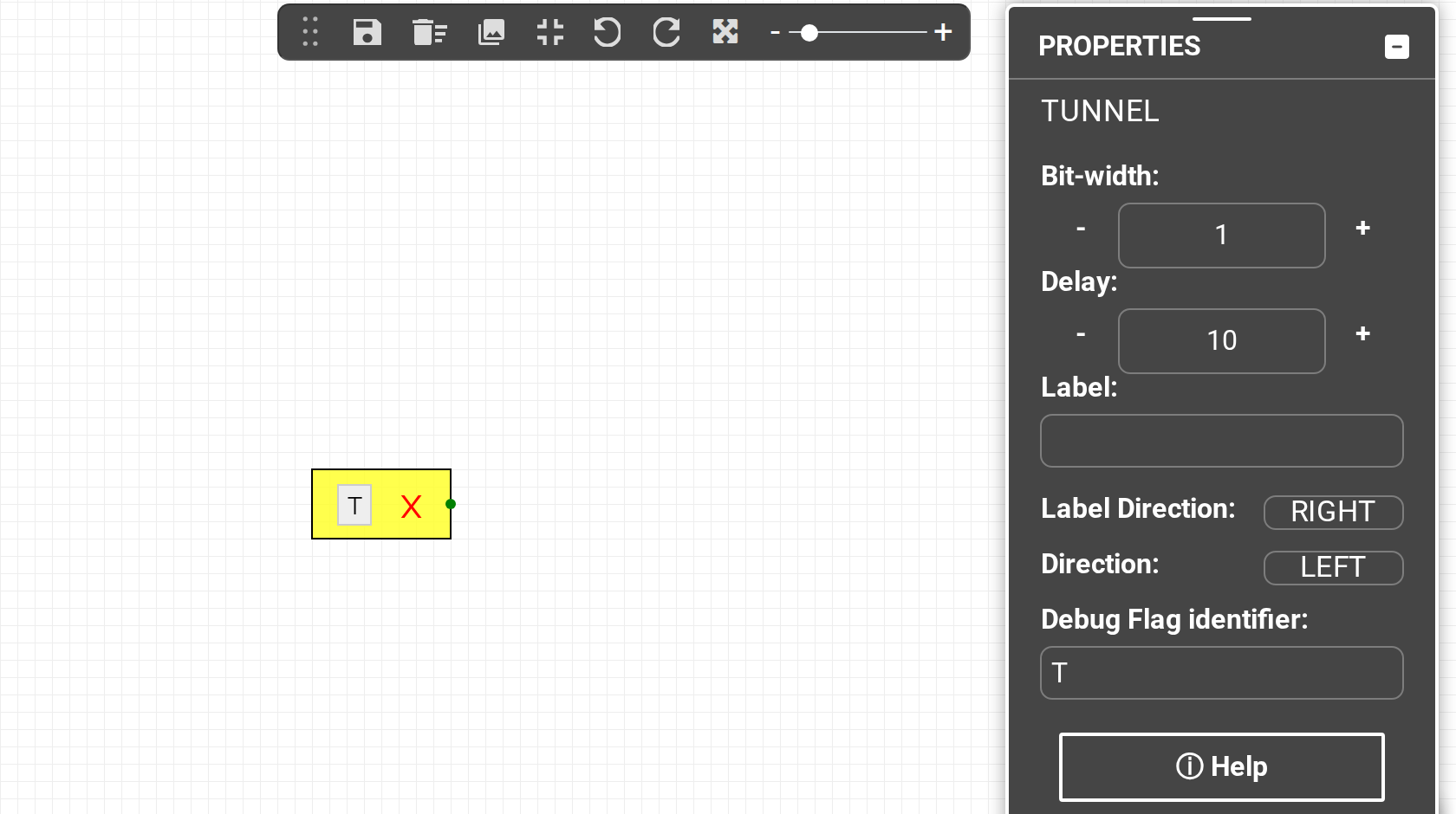
When the Tunnel circuit element is implemented in a circuit design, tunnels with the same Debug Flag identifier attribute (available in the PROPERTIES panel for the Tunnel circuit element(refer Figure 4.18)) are connected together.
Properties that can be customized in the PROPERTIES panel include: BitWidth, Direction, Debug Flag identifier
You can verify the behavior of the Tunnel circuit element in the live circuit embedded below:
Splitter
Splitters split high bitwidth wires (buses) into lower bitwidth wires(buses) and vice versa. It is the only two-way circuit element in LogicPlot.
The bitwidth may be split into equal parts or unequal parts. Consider that you have a 4 bitwidth bus. You may split it into equal or unequal parts as shown below:
- Equal parts: 4 -> 1 1 1 1
- Unequal parts: 4 -> 1 2 1
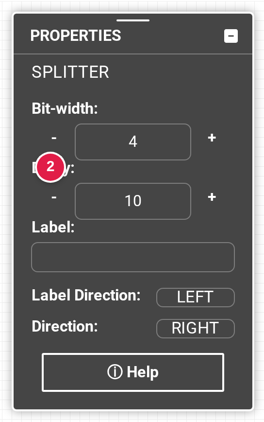
Figure 4.21 shows the relevant properties for a 4 bitwidth splitter split into equal parts.
Properties that can be customized in the PROPERTIES panel include: Direction
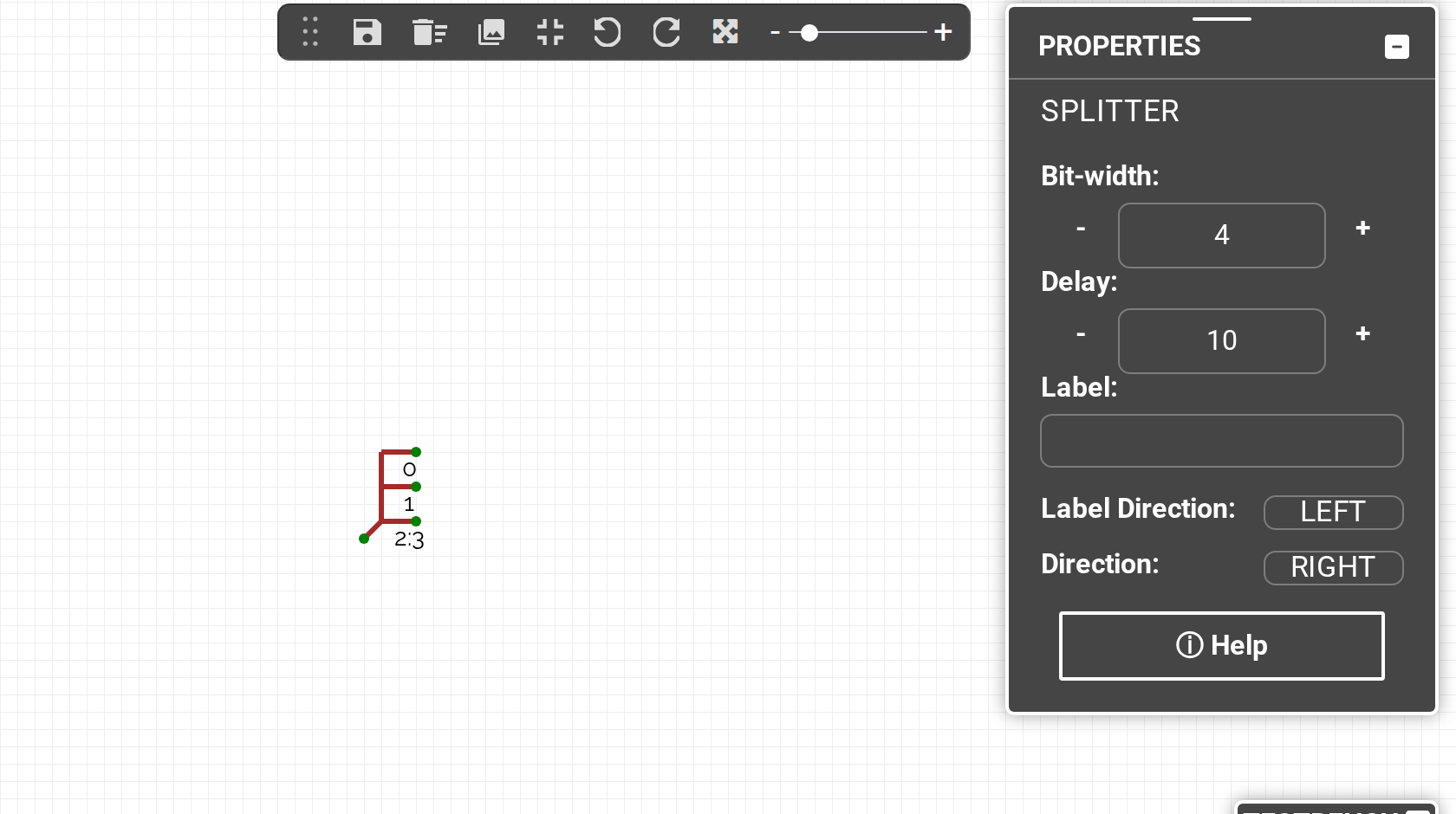
When the Splitter circuit element is dragged on the Canvas, the bitwidth window pops up (refer Figure 4.22) where the user must first identify the total bits the bus.
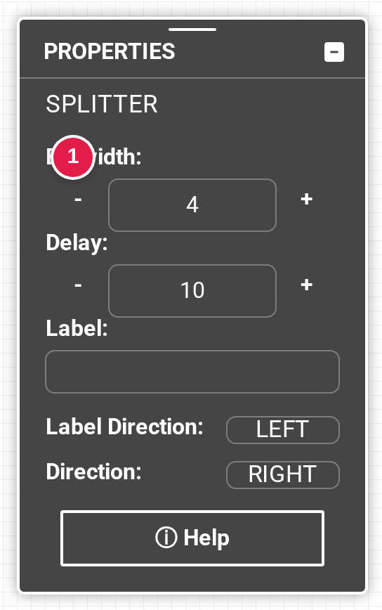
In the follow up window, the user can then identify if the bitwidth must be split into equal or unequal parts.
Equal Split
You can verify the behavior of the Splitter circuit element when the bitwidth is split in equal parts in the live circuit embedded below:
Unequal Split
You can verify the behavior of the Splitter circuit element when the bitwidth is split in unequal parts in the live circuit embedded below:
Flag
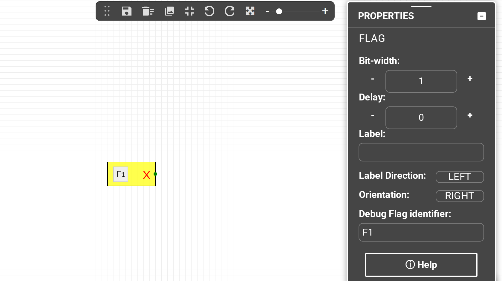
The Flag circuit element is used in a circuit design to flag outputs at different points in your circuit. Figure X highlights the different attributes that are available for this circuit element.
Properties that can be customized in the PROPERTIES panel include**: **BitWidth, Orientation, Debug Flag identifier**
Two's Complement
The Two’s Complement circuit element calculates the two’s complement of any binary number. A two's complement operation is simply a one's complement operation followed by the addition of 1 to the result.
Given number        1  1  1  1  0
1's complement      0  0  0  0  1
add 1               +           1
                   ---------------
2's complement      0  0  0  1  0
You can verify the behavior of the Two’s Complement circuit element in the live circuit embedded below: